OPTOHYB
General information

Perovskite/GaAs hybrid structures: towards enhanced optoelectronic properties

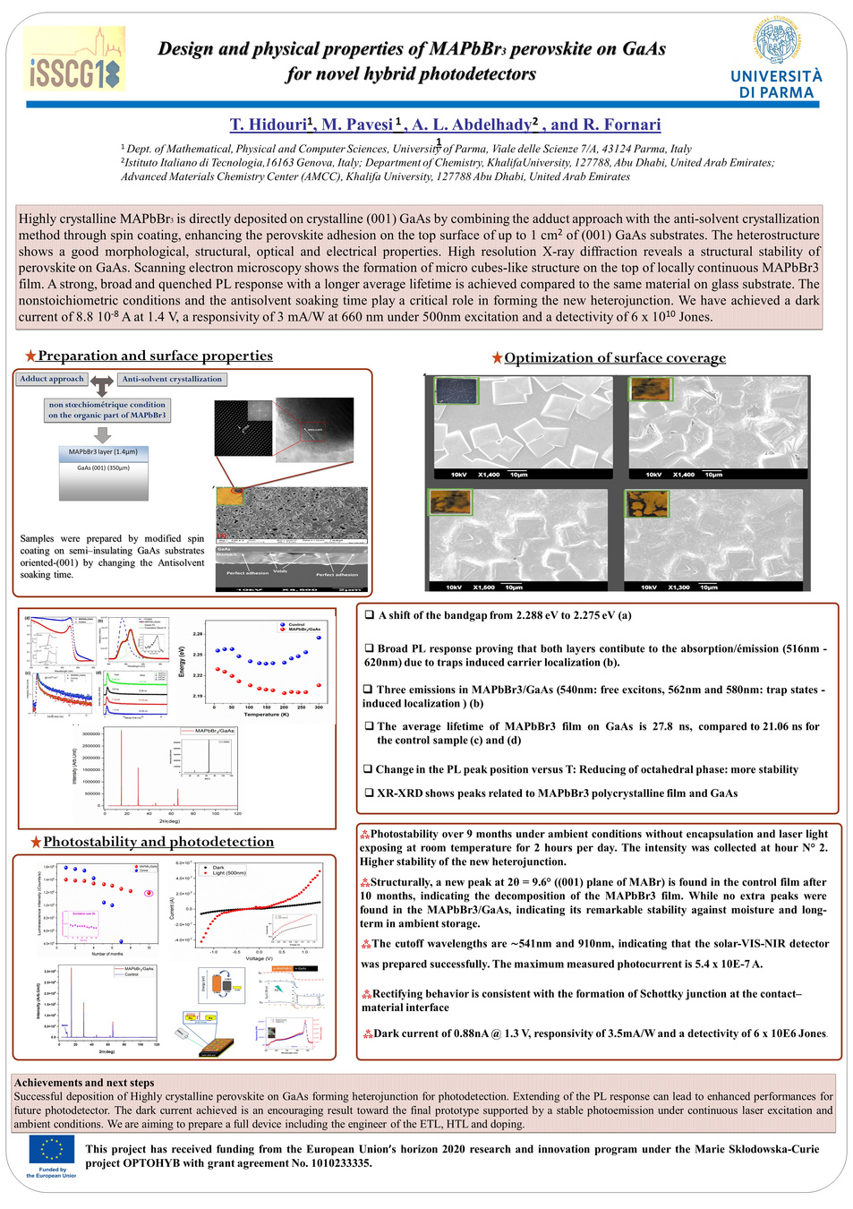
OPTOHYB focuses on studying the carrier localization (CL) in a new hybrid structure namely halide perovskites/GaAs for
photodetection application. Understanding the CL phenomenon in this hybrid structure could provide insights towards
enhancing/controlling the optoelectronic properties. The idea consists of detecting and controlling the CL in the hybrid
heterojunction and orient it towards photodetection devices. The phenomenon can be generated, either, randomly by strain,
composition, size, and diffusion fluctuations, or, controllably by doping. The CL affects the bandgap (creating band-tails
states and optical transitions) which affects the carrier lifetime. The experimental treatment of the phenomenon will be
performed optically by the mean of steady-state photoluminescence (PL) and the time-resolved photoluminescence (TRPL)
to evaluate the CL signatures. The obtained results will be correlated with morphological and structural observations to
qualitatively understand the luminescence mechanisms in the new hybrid structure. To realize OPTOHYB's goal, for the first
time, a quantitative study by modeling the PL features and the decay time will be performed using the Localized State
Ensemble model (LSE) and the generalized model for TRPL. The newly obtained parameters will allow the control of the
CL's evolution versus the ex- and/or in-situ conditions. The successful execution of this proposal will create a new platform
with controllable band-tail state formation and carriers dynamic related to the CL phenomenon. Therefore, slowing the
charge carrier lifetime due to the carrier hopping between different states in the band-tail, which is beneficial for
photodetection. Finally, the fabrication of a photodetector based on halide perovskites/GaAs heterostructure prototype will be
performed. The efficiency of the prototype will be checked regarding the possible engineering of the CL and its effect on the
prototype and the way on how we can exploit it.

This project has received funding from the European Union’s horizon 2020 research and innovation program under the Marie Skłodowska-Curie project OPTOHYB with grant agreement No. 1010233335.

Experienced Researcher
Dr. Tarek Hidouri is originated from Tunisia. Currently, he is serving as an MSCA Experienced Researcher at the Department of Mathematical, Physical and Computer Science, University of Parma, Italy. He graduated in fundamental physics at University of Monastir, Tunisia, with a Master degree in Quantum physics and a thesis in the field of Sciences and Technology focused on physics of materials and photonics. He participated in many conferences and scientific events, and he is serving as a peer reviewer for many journals such as Materials, Vacuum, Optical materials and Applied Physics A. He joined the Italian Institute of Technology (IIT) as an experienced researcher (ER) through the Marie Skłodowska-Curie actions and then as an ER under the same framework at Parma University. He is serving as a leader of many scientific projects in China, Italy and Saudi Arabia.
The research activities of Dr. Tarek Hidouri are mainly focused on the preparation and optical characterization of new class of semiconductor materials for optoelectronic applications. The global aim of his research is elaborating/structuring new materials at the nanoscale which will open new possible applications such as photodetectors, LEDs and solar cells.
Supervising in UNIPR
Pr. Roberto Fornari graduated in physics at the University of Parma in 1980.
From 1981 to 2003 he worked as research scientist at the Institute for Electronic and Magnetic Materials (IMEM, former MASPEC) of the Italian National Research Council where he led different research projects on growth and characterization of compound semiconductors.
From 2003 to 2013 he was director of the Leibniz Institute for Crystal Growth (IKZ) in Berlin, with a joint appointment as Full Professor at Technical University of Brandenburg, Cottbus, and later at Humboldt University Berlin.
In 2013 he accepted a call from the University of Parma where he currently holds the Chair of Materials Physics at the Dept. of Mathematical, Physical and Computer Sciences. He has been Coordinator of the Physical Section of the Dept., and is presently Vice-Rector for Research at Parma University.
Roberto Fornari has authored/co-authored about 250 scientific papers, nine patents and different chapters on crystal growth and properties of technologically important materials. The actual scientific interests are focused on wide bandgap and oxide semiconductors.
He has edited books and proceedings on crystal growth and materials science, and is presently member of the editorial boards of J. Crystal Growth, Discover Materials, Cryst. Res.Technol., J. Optoelectronics and Advanced. Materials.
He has served in many scientific bodies, commissions, conference committees and evaluation panels. He was President of the International Organisation for Crystal Growth (IOCG) from 2010 to 2016 and member of the Executive Committee of European Materials Research Society (E-MRS) from 2011 to 2017.
Supervising in IIT
Dr. Ahmed Abdelhady holds a PhD degree in Chemistry from The University of Manchester – (United Kingdom). Currently, he worked as a Researcher at the Nanochemistry department at IIT (Italy), and previously he was a Postdoctoral-Fellow at King Abdullah University of Science & Technology (KAUST) – Saudi Arabia. As a researcher, he leads a group focusing on halide perovskite thin films and single crystals for optoelectronic applications. Since 2012, He has worked and collaborated with renowned research groups in the field of halide perovskites including Sargent’s group (University of Toronto), Bakr’s group (KAUST), Dowben’s group (University of Nebraska-Lincoln), Goriely’s group (University of Oxford), Loo’s group (Princeton University), as well as Manna and Petrozza groups (Istituto Italiano di Tecnologia). He has developed new crystallization techniques for perovskite single crystals, namely, inverse temperature crystallization (ITC) and solvent acidolysis crystallization (SAC). His work has contributed greatly to the perovskite research focusing on the fabrication of high sensitivity photodetector, UV photodetectors, and bifunctional photodetectors.



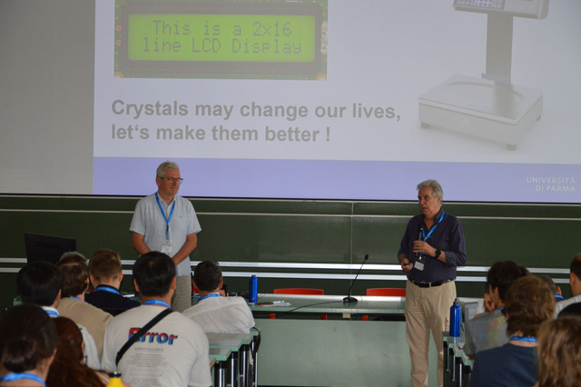
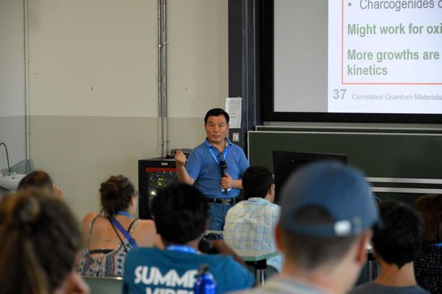
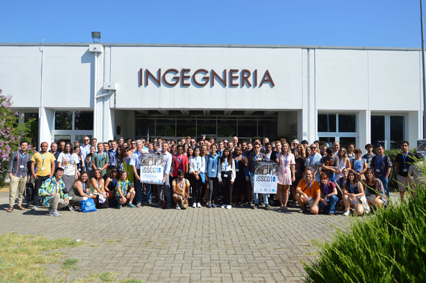
ISSCG18
Summer school
And more on ...



Scientific production
processing ...

